Ceramic nanofibers offer a pathway to more efficient, durable and environmentally friendly manufacturing processes. For instance, rare-earth elements are often used to process exhaust gas in catalytic converters.
Using rare-earth materials in nanofiber forms reduces the required quantity significantly by increasing the surface area tens of thousands of times compared to the current form used in catalytic converters.
Similarly, in energy storage and conversion devices, such as fuel cells, the use of ceramic nanofibers could lead to more compact, efficient and longer-lasting systems, accelerating the transition to renewable energy sources.
Their role extends to critical applications in radiation shielding for spacecraft, enhancing the safety and longevity of missions in the harsh environment of space. The versatility of ceramic nanofibers is further demonstrated in their application within filtration and membrane technology, where they improve the efficiency and durability of filtration systems. Different types of biomaterials made of ceramic nanofibers have been studied for wound healing and bone tissue regeneration, with numerous advances in this material development.
The integration of ceramic nanofibers into new and existing products will not only enhance performance but also enable the development of technologies that were previously considered impractical or too costly.
Fermilab researchers are investigating the use of ceramic nanofibers as target materials in high-energy particle physics experiments, addressing challenges encountered by bulk solid materials in subatomic particle production. Batavia, Illinois, is a United States Department of Energy national laboratory specializing in high-energy particle physics.
In these experiments, Fermilab used a high-intensity focused pulsed proton beam, which heats a small area of the target that expands rapidly during a short time. This gives rise to compressive stress waves, which may lead to high cycle fatigue and other radiation damage in bulk solid materials. This may result in premature failures of targets material and beam intercepting devices used for sub-atomic production, increased maintenance expenses and interruptions in physics experiments.
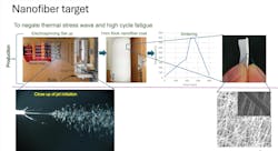
Nanofibers promise to solve the problem of thermal shock, compressive stress wave, high cycle fatigue as well as radiation damage, which are prevalent in currently used solid targets. Since the diameter of nanofiber is much smaller than the beam spot size, there will be no macroscopic thermal gradient across a single nanofiber. Additionally, numerous gaps exist between the adjacent nanofibers, effectively inhibiting any type of compressive stress waves. The nanofibers' high surface area and porosity facilitate efficient cooling within the mat, even from the beam center, by circulating helium gas through the porous target.
The submicron diameter and prevalent grain boundaries of nanofibers decrease the mean free path for low-solubility transmutation products, such as helium gas formed from proton beam interaction with the material. This facilitates their escape from the solid, thereby preventing swelling and subsequent cracking in the bulk material.
Unlike a bulk solid material where localized damage could lead to catastrophic failure of an entire target structure, the nanofiber mat can maintain its integrity even if there is local damage of a few nanofibers.
Electrospinning Process Explained
Creating ceramic nanofibers involves a process known as electrospinning. It begins by preparing a desired ceramic compound in an appropriate solvent and then loading it into a syringe.
The process entails applying a high voltage to the needle, while maintaining a grounded metal collector plate in front of the syringe needle at a specific distance to maintain a high-electric field gradient. When the solution exits the needle, it forms a droplet. The concentration of electrical charge on the droplet's surface induces a force that overcomes the surface tension, causing the droplet to elongate under the electric field's influence and form a liquid jet accelerating toward the collector plate.
Further jet stretching and solvent evaporation leads to the formation of solid fibers with a diameter of less than one micrometer by the time it reaches the collector plate. This process forms a nonwoven fiber mat. The next step involves baking the fiber mats in a high-temperature oven while following a specific heating profile to eliminate the polymer part, so only the ceramic material is present.
While significant research has been conducted on electrospinning polymeric nanofibers, comparatively less attention has been devoted to the production of ceramic or metallic nanofibers, particularly in enhancing their thermal, mechanical and radiation resistance properties.
In many industrial applications, the ceramic nanofiber mat is very thin and structural integrity of the fiber mat isn’t a factor. However, for target materials in high-energy science experiments and medical isotope production, standalone, thicker nanofiber mats are required. That’s because they must be capable of enduring radiation damage and thermal shock caused by intense pulsed beams.
Although electrospinning is an easy way to produce a wide variety of nanofibers, the production rate is extremely slow. This limited the application of ceramic nanofiber from the lab to industrial scale. The innovation introduced by Fermilab through a patented electrospinning process addressed the problem of fabricating thicker ceramic nanofiber mat at high production rate.
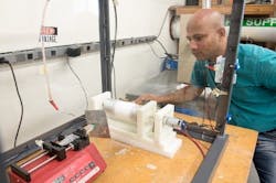
We used a custom-made, low-power output high-voltage source for electrospinning setup. The process is designed to be cost effective and compact, while providing much more electrical safety during operation than other electrospinning techniques. It involves a unique configuration using a negative ionizer, a customized profiled electrode employing a free-surface electrospinning technique and a compact, high-voltage unit. This process can help increase nanofiber production output while achieving desired thickness levels.
To demonstrate the resilience of ceramic nanofibers against radiation damage, zirconia fibers, created at Fermilab, underwent irradiation using low-energy heavy ions—specifically, 1 MeV krypton ions in-situ transmission electron microscopy at Argonne National Lab.
The study showed the absence of dislocation clustering, voids and any noticeable change in crystal lattice parameters. This suggests that the nanofibers are resistant to dislocation formation, owing to the presence of nanopolycrystalline microstructures. The nanofibers also included a plethora of grain boundaries and free surfaces that act as sink sites to such displacement damages.
To demonstrate nanofiber mats’ ability to negate the adverse effects of beam-induced compressive stress waves (Figure 1), Fermilab subjected the mats to rigorous testing using intense pulsed beams at the CERN HighRADMat facility in Switzerland.
While the mats demonstrated resilience, their performance exhibited a degree of dependency on the packing density of the nanofiber. Presently, an investigation is underway to understand the heat and mass flow within these ceramic nanofiber mats and to determine optimal packing densities and fiber diameters required for survival under high-energy proton beams.
One of the drawbacks of using a nanofiber mat in physics experiment is their low overall density, which adversely affects the yield of subatomic particles generation. To tackle this problem, Fermilab is producing high-density material, such as tungsten nanofiber, using the electrospinning process.
Following successful demonstrations of radiation-resistant ceramic nanofibers produced via the electrospinning technique, attention is now directed toward scaling the production process and further refining the properties of these nanofibers to align with specific industry needs.
Study Outcomes and Potential
Collaborations with international research centers, such as CERN – the European Organization for Nuclear Research – where functional nanofibers are already being utilized for medical isotope production, are in progress. CERN is exploring ways to enhance the service life of such nanofibers and to produce tailored nanofibers for specific medical isotopes production. Fermilab also has demonstrated that its setup can be used for mass production of polymer nanofiber for other consumer goods applications, such as air filters.
This application requires only a thin layer of nanofiber coating on filter substrate with a low-efficiency rating. Efforts continue at Fermilab to optimize both the fiber diameter and layer thickness. The goal here is to reduce air flow resistance through the filter media, all the while preserving a high filtration efficiency for sub-micron particles.
The research at Fermilab, which resulted in the development of an electrospinning technique for manufacturing ceramic nanofibers, marks a major advancement in materials science. This innovation has the potential to drive transformative changes across various industries by enhancing accessibility and affordability of advanced materials.
The work at Fermilab to develop an electrospinning technique for producing ceramic nanofibers represents a significant milestone in materials science. By making these advanced materials more accessible and affordable, this innovation holds the potential to drive transformative changes across a wide range of industries. As we stand on the brink of a new era in materials technology, the continued exploration and application of ceramic nanofibers will undoubtedly unlock new possibilities for a sustainable and technologically advanced future.


