Nanorods Boost Boiling
Depositing copper nanorods on a copper surface significantly enhances boiling, say researchers at Rensselaer Polytechnic Institute (http://www.rpi.edu/), Troy, N.Y. “The increased boiling efficiency seems to be the result of an interesting interplay between the nanoscale and microscale surfaces of the treated metal,” notes Nikhil Koratkar, associate professor in the school’s department of mechanical, aerospace and nuclear engineering. Other metals and metalloids like silicon may provide similar results, he adds.
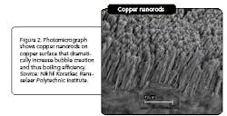
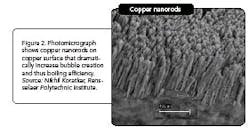
Tests were conducted with 1-in. × 1-in. wafer covered with nanorods via oblique-angle deposition. The nanorods’ height was about 450 nm and the tip-to-tip spacing between them was around 50 nm.
While the technique ultimately may lead to better energy efficiency in industrial heat exchangers, Koratkar foresees the most immediate potential for taking care of hot spots on microelectronic circuits. He’s already talking to some chipmakers and hopes to start tests within the next year. He also aims to explore whether a thin hydrophobic layer on the nanorods will provide even greater bubble density and to investigate the effect of rod height, spacing and orientation.
Robustness of the rods may need attention, he admits. In the tests after five to 10 cycles, some aging or deterioration occurred. So, he also plans to explore alternatives to create more robust rods.

